A Graphics Processing Unit (GPU) is a specialized electronic circuit originally designed to accelerate the rendering of images for output to a display.
Unlike a Central Processing Unit (CPU), which is optimized for sequential serial processing, a GPU is built around a highly parallel architecture, enabling it to process many operations simultaneously. This parallelism is facilitated by a many-core microprocessor design and high-bandwidth private memory, allowing for efficient execution of numerous simultaneous threads. The typical GPU architecture supports fine-grain SIMD (Single Instruction, Multiple Data) parallelism, which enables the execution of the same operation across multiple data points in parallel. Additionally, GPUs are characterized by low-latency floating-point computations, making them particularly effective for operations involving complex mathematical models and transformations.
The emergence of GPUs was largely driven by the increasing demand for high-resolution 3D graphics rendering in video games and other visually intensive applications. Rendering a 3D scene requires performing linear algebra operations—such as matrix multiplications and vector transformations—on millions of vertices and pixels in real-time, often at frame rates exceeding 60 frames per second (FPS). Since each vertex or pixel can be processed independently, the workload is inherently parallel, making GPUs ideally suited for such tasks. To efficiently manage this parallel workload, modern GPUs deploy thousands of lightweight threads that execute concurrently, each handling a small part of the data independently but synchronously.
Under Flynn’s taxonomy, which categorizes computer architectures based on instruction and data streams, GPUs fall into the SIMD category. This means they execute a single instruction across multiple data elements simultaneously, optimizing them for data-parallel computation. This architectural paradigm allows GPUs to achieve high throughput on tasks involving repetitive, parallel operations, such as those found in scientific computing, deep learning, and graphical rendering.
Architectural Differences Between CPU and GPU
While both CPUs and GPUs serve as processors, they are architecturally and functionally distinct, each optimized for different types of workloads.
CPUs are designed with the goal of minimizing latency for a broad range of tasks, which often involve complex logic and sequential control flow. To achieve this, CPUs are equipped with sophisticated control logic, large caches, and a relatively small number of powerful cores optimized for single-threaded performance.
GPUs, in contrast, prioritize throughput over latency. This means they are optimized to maximize the amount of work done over a given period, rather than the speed of any individual task. A GPU comprises hundreds or thousands of simpler cores and includes pipelined Arithmetic Logic Units (ALUs) with high throughput capabilities, even if individual instructions may experience longer latency. This design enables GPUs to excel in massively parallel workloads, where the same operation is applied to many data elements concurrently.
Memory architecture also differs significantly. GPUs typically have high-bandwidth memory subsystems, albeit with smaller caches, which support the rapid movement of large volumes of data—a crucial feature for applications like matrix operations in machine learning. Additionally, GPUs feature simple control logic and lightweight thread scheduling, which facilitates rapid context switching and the ability to hide memory access latencies through multithreading.
Over the years, GPUs have evolved beyond their original role in graphics rendering to become general-purpose parallel processors, a transition often referred to as GPGPU (General-Purpose computing on GPUs). Today’s GPUs can be programmed using high-level languages such as CUDA (for NVIDIA GPUs) or OpenCL, and support IEEE 754-compliant floating-point arithmetic in both single and double precision, making them suitable for scientific and engineering applications.
NVIDIA GPU Architecture
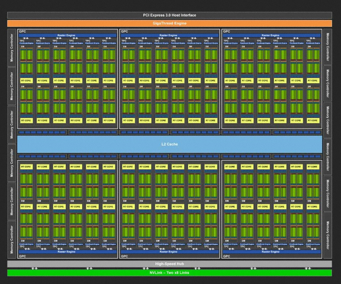
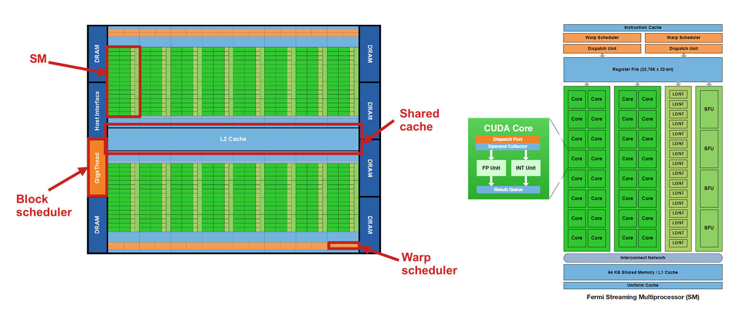
NVIDIA, one of the leading manufacturers of GPUs, has developed several GPU architectures tailored for high-performance computing and machine learning. A typical NVIDIA GPU consists of two main components: the Global Memory and the Streaming Multiprocessors (SMs).
The Global Memory of NVIDIA GPUs ranges between 16 and 40 GB, depending on the model, and employs high-bandwidth technologies such as GDDR5, HBM2 (High Bandwidth Memory), and interfaces like PCIe (Peripheral Component Interconnect Express) to enable data transfer speeds as high as 1600 GB/s.
Each Streaming Multiprocessor contains a variety of computational units including numerous ALU cores (often over 100), floating-point units, logical units (for basic operations such as addition, subtraction, and multiplication), and specialized units for comparison, data movement, and branching. The SM also contains a large register file (ranging from 32K to 64K registers), a fast-access shared memory, and instruction dispatch units that manage the execution of threads efficiently.
The evolution of NVIDIA’s GPU models reflects substantial improvements in raw computing power. For example:
Model
FP32 TFLOPS
Cores
RAM
Bandwidth
Link
Kepler K40
4.29
2880
12 GB DDR5
240 GB/s
PCIe3.0x16
Pascal P100
10.6
3584
16 GB HBM2
732 GB/s
PCIe3.0x16
Volta V100
15.7
5120
32 GB HBM2
900 GB/s
PCIe3.0x16
Ampere A100
19.5
6912
40 GB HBM2
1600 GB/s
PCIe4.0x16
These GPUs are not only used in gaming but are central to modern AI training pipelines, scientific simulations, and big data analytics due to their unparalleled ability to handle large-scale matrix and tensor operations.
Comparison Between GPUs and Vector Processors
Both GPUs and Vector Processors are tailored for data-parallel workloads, where the same operation is applied across large datasets. These architectures share several features: they both utilize scatter-gather data transfers, mask registers for controlling conditional operations, and large register files to support high-speed computation.
However, key architectural differences set them apart. A notable distinction is that Vector Processors usually include a scalar processor, which handles control logic and scalar computations, alongside vector processing units. GPUs, on the other hand, lack dedicated scalar units and instead rely on multithreading to hide memory latency, using thread-level parallelism to ensure computation continues even when some threads are waiting for memory access.
Another difference lies in the number of functional units. Vector processors generally have a small number of highly optimized, fully pipelined units, whereas GPUs are designed with a vast number of simpler functional units, enabling them to achieve a much higher degree of parallelism. This architectural decision allows GPUs to perform many operations concurrently, making them extremely effective for throughput-intensive applications, especially where computation can be partitioned into many small, independent tasks.
General-Purpose GPU (GPGPU) Computing
In the realm of high-performance computing, numerous scientific and technical applications—ranging from image and signal processing to numerical simulations and large-scale scientific computations—are characterized by their need to process vast quantities of data with high computational intensity. These applications often exhibit a high degree of data parallelism, making them suitable candidates for acceleration via GPUs. The concept of General-Purpose GPU (GPGPU) computing emerges from the attempt to repurpose GPUs, originally designed for rendering 3D graphics, for the execution of general-purpose computational workloads that benefit from parallel execution.
GPGPU computing harnesses the architecture of GPUs, which is inherently optimized for parallel processing, to perform computations that would traditionally be executed on CPUs. This architectural distinction makes GPUs especially powerful for workloads characterized by a high volume of uniform mathematical operations on large datasets, where control flow divergence is minimal and synchronization requirements are limited.
In GPGPU architecture, the CPU (often referred to as the host) and the GPU (the device) function in tandem. Each has its own memory space: the CPU accesses its standard system memory, while the GPU has access to high-bandwidth memory that supports the large-scale, parallel access patterns typical of data-intensive applications. The CPU handles the orchestration of tasks, managing logic-heavy, serial, or event-driven portions of the program. The GPU, in contrast, executes massively parallel computations, enabling dramatic acceleration of workloads that would otherwise be computationally expensive if run solely on the CPU.
The CPU and GPU are optimized for distinct operational paradigms. CPUs are well-suited for workloads involving low-latency, cached data access and sophisticated control logic, due to features such as out-of-order and speculative execution. GPUs, by contrast, are optimized for high-throughput computing and excel at hiding memory latency through massive parallelism and multithreading.
The collaboration between CPU and GPU typically follows this division of labor:
CPU: Manages serial execution, coordinates program flow, handles I/O and event-driven logic, and prepares data structures for GPU processing.
GPU: Executes compute-intensive, data-parallel workloads that benefit from SIMD-style execution across thousands of threads.
GPGPU Programming Model
The GPGPU programming model typically follows a structured workflow in which computationally intensive sections of an application are offloaded to the GPU:
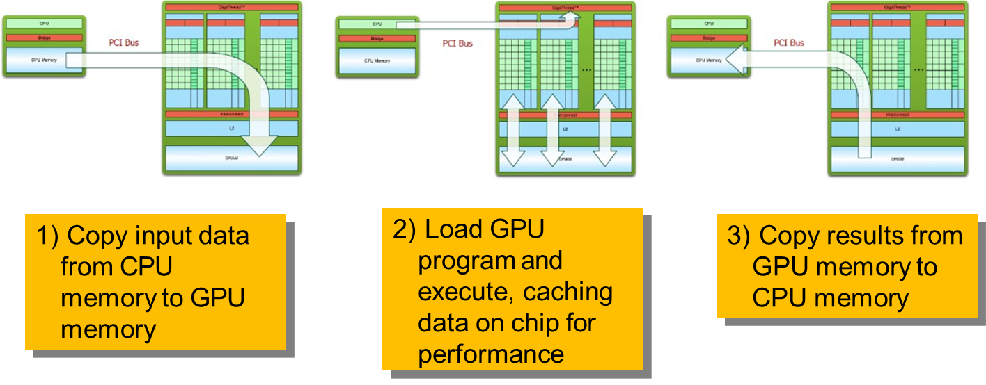
Memory Transfer (Host to Device): Input data is transferred from the CPU’s memory to the GPU’s global memory via the PCI Express (PCIe) interface.
Kernel Execution: The GPU executes parallel code—referred to as a kernel—on the data, exploiting shared memory and registers for performance optimization.
Memory Transfer (Device to Host): After execution, the results are copied back from GPU memory to CPU memory for further processing or output.
Despite the GPU’s superior compute capabilities, a notable limitation arises from the bottleneck associated with data movement between the CPU and GPU. The PCIe bus, while offering high bandwidth relative to standard I/O, is still slower than the internal memory bandwidth of CPUs and GPUs. Consequently, inefficient data transfer patterns can nullify the computational gains of GPU acceleration. Careful consideration of data locality and memory management is thus essential when porting CPU-bound applications to GPGPU platforms.
To mitigate data transfer overhead, modern GPU programming environments provide abstractions and tools to reduce, hide, or automate memory transfers, allowing developers to focus on computation and optimization rather than low-level memory management.
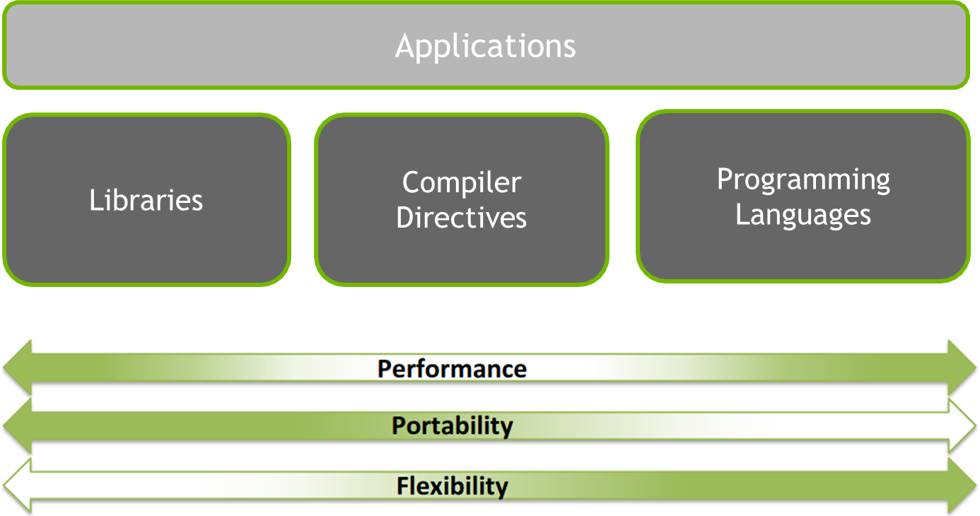
High-Level Tools and Abstractions
Several programming tools and models have emerged to simplify GPGPU development and bridge the gap between performance and programmability:
Libraries
Highly optimized GPU-accelerated libraries offer a convenient and efficient means to perform complex computations without requiring low-level GPU programming. These libraries encapsulate domain-specific operations and provide interfaces that abstract GPU execution.
Example
cuDNN, TensorRT, DeepStream SDK for deep learning workloads.
cuBLAS, cuSPARSE, cuSOLVER for dense and sparse linear algebra.
cuFFT, NVIDIA NPP, CODEC SDK for signal processing and image/video transformations.
nvGRAPH, NCCL, Thrust for graph analytics and parallel primitives.
Compiler Directives
Compiler directives offer a high-level, declarative approach to parallelism by annotating existing C or C++ code with pragmas that guide the compiler in generating parallel GPU code. This approach is less intrusive and enhances portability.
For example, the OpenACC model allows specifying parallel loops for GPU execution:
// CPU code#pragma omp parallel for reduction(+:pi)for (int i = 0; i < n; i++) { double t = (double) ((i + 0.05) / N); pi += 4.0 / (1.0 + t * t);}// GPU code#pragma acc parallel loop reduction(+:pi)for (int i = 0; i < n; i++) { double t = (double) ((i + 0.05) / N); pi += 4.0 / (1.0 + t * t);}
This is analogous to OpenMP for CPUs and is designed to ease the migration of serial applications to parallel environments.
Programming Languages and Frameworks
For full control over performance and architectural features, developers can use dedicated GPU programming languages or APIs such as CUDA, OpenCL, and SYCL. These platforms allow direct implementation of GPU kernels and provide fine-grained control over memory hierarchy, thread synchronization, and execution configuration.
Popular programming interfaces include:
CUDA C/C++: Proprietary language extension by NVIDIA, offering the richest access to GPU features.
OpenCL: Open standard for heterogeneous computing, supporting a wide variety of devices.
SYCL and OneAPI: Modern C++-based models supporting cross-platform heterogeneous programming.
Hybrid solutions: Languages like Python (with PyCUDA, Numba), C# (Hybridizer), or numerical tools (MATLAB, Mathematica) that provide GPU capabilities via high-level interfaces or bindings.
CUDA Fundamentals
Definition
CUDA, an acronym for Compute Unified Device Architecture, is a parallel computing platform and programming model developed by NVIDIA. It is designed to enable software developers to exploit the massive parallelism inherent in modern NVIDIA Graphics Processing Units (GPUs).
Unlike traditional programming paradigms restricted to CPUs, CUDA allows developers to write C, C++, or Fortran code that directly runs on the GPU hardware. The fundamental premise of CUDA is to simplify GPU programming by abstracting low-level hardware complexities, thereby making general-purpose GPU programming more accessible, even to those without prior experience in graphics programming.
The core idea behind CUDA is to expose the GPU’s large number of cores as independent threads that can be executed concurrently. CUDA follows the Single Instruction, Multiple Thread (SIMT) execution model, which is conceptually similar to SIMD (Single Instruction, Multiple Data), but designed to be more flexible. In SIMT, thousands of threads execute the same kernel function but operate independently on different pieces of data. This makes CUDA highly effective for data-parallel workloads, such as image processing, matrix operations, and deep learning computations.
A CUDA program is typically structured such that the computationally intensive portion of the code is offloaded to the GPU, while the CPU orchestrates the flow of the application and performs tasks that are either inherently sequential or involve control-heavy logic. The GPU-executed function is called a kernel. When a kernel is launched, it is instantiated across a large number of lightweight threads, each responsible for computing a small, independent part of the overall problem.
Example
Consider a simple operation like vector addition. In a traditional CPU implementation, a loop iterates over each element of the vectors and performs addition sequentially. In contrast, the CUDA version launches a kernel where each thread is assigned to compute a single element of the output vector, all in parallel. The CUDA version requires the programmer to retrieve the thread’s unique ID—typically derived from its block and thread indices—to access the appropriate data element:
// CPU implementationvoid vsum(int* a, int* b, int* c){ for (int i = 0; i < N; i++){ c[i] = a[i] + b[i]; }}void main(){ int va[N], vb[N], vc[N]; //... vsum(va, vb, vc);}// ------------------------------------------// CUDA kernel__global__void vsum(int* a, int* b, int* c){ int i = threadIdx.x; // get thread index within the block c[i] = a[i] + b[i];}void main(){ int va[N], vb[N], vc[N]; //... vsum <<<1, 1>>>(va, vb, vc); // launch kernel with 1 block // and 1 thread}
Launching a kernel on the GPU is done using the <<<...>>> syntax, where the programmer specifies the number of blocks and threads per block. In the simplest form, one might launch a kernel with a single block and a single thread, although practical applications typically involve multiple blocks and hundreds or thousands of threads per block to exploit the full computational potential of the GPU.
CUDA’s execution model is built on a hierarchical thread structure, which mirrors the physical and architectural design of NVIDIA GPUs. Threads are organized into blocks, and blocks are further organized into grids. This hierarchy facilitates scalable execution across different generations of GPU hardware. Each block is executed on a single Streaming Multiprocessor (SM), a fundamental unit within the GPU responsible for managing instruction execution and resource allocation for threads.
Threads within the same block can collaborate and share data via shared memory, a fast, user-managed cache that enables efficient intra-block communication. Furthermore, the hardware executes threads in units called warps, each consisting of 32 threads. Threads in a warp execute instructions in lockstep unless control divergence occurs, which can impact performance. CUDA’s hardware and software scheduling infrastructure can dynamically map blocks to SMs, allowing blocks to be interleaved and executed concurrently to maximize GPU resource utilization.
The hierarchical thread model offers several advantages. It enhances scalability, allowing the same program to run efficiently on GPUs of different sizes by adjusting the number of blocks and threads per block. It also provides modularity, enabling structured parallel programming through division of labor among threads and blocks. Additionally, this hierarchy supports local cooperation among threads (within a block) and global coordination (across the grid), which are essential in more advanced CUDA applications involving synchronization, tiling, and complex memory access patterns.
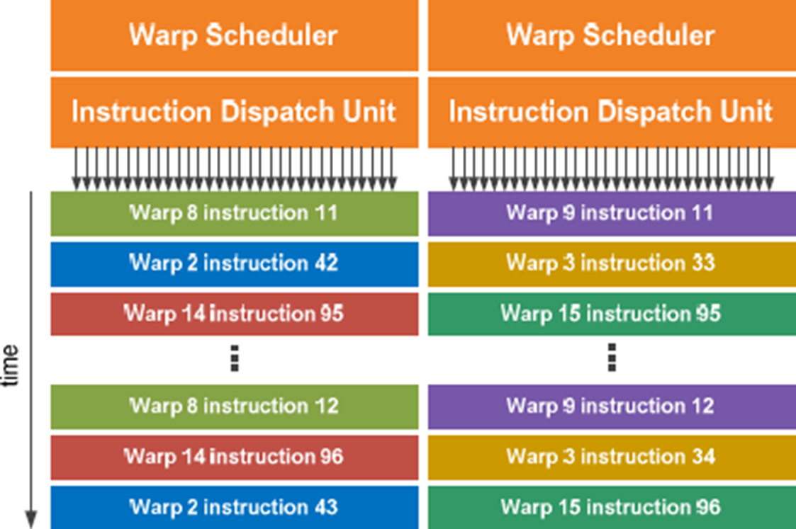
Warp Scheduling in CUDA Architecture
In CUDA-enabled NVIDIA GPUs, warp scheduling is a central concept that governs how threads are executed in parallel on the device. Rather than scheduling individual threads, the GPU schedules groups of 32 threads, collectively referred to as a warp. These threads execute in a lockstep fashion, meaning they all perform the same instruction at a given time, albeit on different data. This model corresponds to the Single Instruction, Multiple Thread (SIMT) paradigm, which is distinct from SIMD in that SIMT allows each thread to maintain its own register state and follow divergent control paths, albeit with performance trade-offs.
Each Streaming Multiprocessor (SM) contains a warp scheduler responsible for issuing instructions to the execution units. Multiple warps may reside on a single SM concurrently, and the warp scheduler dynamically selects which warp to execute next based on thread readiness and data availability. This form of fine-grained multithreading allows the GPU to hide memory latency and keep the execution units fully utilized by switching between warps as necessary. By grouping threads into warps, the GPU achieves high throughput for data-parallel tasks while reducing the overhead associated with control flow and instruction decoding.
CUDA Execution Model
When a kernel function is launched, it is instantiated across a multidimensional grid of thread blocks. Each thread block is allocated to an available Streaming Multiprocessor, which manages its execution independently.
Within a block, threads are further divided into warps, the fundamental scheduling units of execution. The SM’s warp scheduler selects one or more warps at each cycle, issues instructions, and manages dependencies and memory accesses. Upon completion of a block’s execution, the runtime system dynamically schedules new blocks to the idle SMs, thereby ensuring continuous workload dispatch and efficient utilization of GPU resources.
This model allows thousands of threads to execute concurrently, provided the problem is decomposed into parallel sub-tasks. Developers must therefore understand both the software and hardware implications of thread, block, and grid organization to fully exploit the computational capacity of the GPU.
Control Flow Divergence
A challenge associated with warp-based execution is control divergence, which arises when threads within a warp do not follow the same execution path due to conditional branching. For instance, when different threads in a warp encounter an if-else condition and evaluate it differently, the warp must execute each control path serially. During this time, threads not on the active path are effectively disabled, leading to serialization of what would otherwise be parallel computation.
Example
To illustrate, consider a warp of 32 threads where some threads satisfy a conditional branch while others do not. The warp will execute the instructions corresponding to one branch while masking out the non-participating threads, and then repeat the process for the other branch.
This behavior reduces the effective parallelism and undermines the performance benefits of SIMT. Divergence is particularly costly when the decision granularity is smaller than the warp size. Conversely, divergence at higher structural levels (e.g., across blocks or grids) does not cause warp-level serialization if each warp follows a consistent control path.
Programmers can mitigate divergence by restructuring control flow to align thread behavior within a warp. For example, using decisions based on blockIdx rather than threadIdx ensures that all threads in a warp or block behave similarly, avoiding divergent execution.
Memory Hierarchy
The CUDA programming model exposes a complex but efficient memory hierarchy designed to balance speed, accessibility, and scope.
At the lowest level, each thread has access to registers, which are high-speed, private storage spaces used to hold local variables and temporary results. Registers are the fastest memory resource available to threads but are limited in size.
Within a block, threads can access shared memory, a user-managed cache that enables fast data sharing and cooperation among threads. Shared memory is physically located on-chip and significantly reduces the latency associated with global memory access. Proper usage of shared memory is critical for optimizing data reuse and minimizing access contention.
At the global level, all threads across all blocks can access global memory, which resides off-chip in the device DRAM. This memory is large in capacity but has relatively high access latency. Because global memory operations are expensive, developers often employ memory coalescing techniques to optimize access patterns and reduce performance penalties.
In addition to these, modern GPUs include L1 and L2 caches that automatically store frequently accessed global memory data. These caches improve effective memory bandwidth and reduce latency, especially in workloads with spatial or temporal locality. Efficient utilization of the memory hierarchy is a cornerstone of high-performance CUDA programming.
NVIDIA Fermi Architecture (2010)
The NVIDIA Fermi architecture, introduced in 2010, marked a significant leap in general-purpose GPU computing. It featured a total of 512 CUDA cores, distributed across 16 Streaming Multiprocessors, each equipped with 32 cores. Each SM also contained two warp schedulers, 16 load/store units, and four Special Function Units (SFUs). These components enabled the simultaneous scheduling of two warps, allowing for greater throughput and better latency hiding.
Fermi was notable for its improved double-precision floating-point performance, support for IEEE 754-2008 compliance, and the inclusion of fused multiply-add (FMA) instructions, which enabled high-performance scientific computing. The architectural pipeline allowed for the execution of two single-precision or one double-precision operation per cycle per core, offering significant compute density for parallel workloads.
The architecture featured a dual-level hardware scheduler: the GigaThread Engine was responsible for distributing thread blocks across SMs, potentially across multiple kernels, while dual warp schedulers handled the intra-SM instruction dispatch for individual warps. This two-tiered system provided flexibility and throughput improvements in dynamic and heterogeneous workloads.
Memory architecture in Fermi also saw notable enhancements. It included 768 KB of L2 cache shared across all SMs, and a 64 KB configurable memory per SM, which could be partitioned between shared memory and L1 cache. The register file supported 32,768 32-bit registers per SM, with up to 64 registers per thread, enabling highly parallel execution with minimal memory latency.
The Evolution of NVIDIA GPU Architectures
Following the Fermi generation, NVIDIA released successive GPU architectures that steadily improved upon performance, efficiency, and programmability.
The Kepler architecture (2012) introduced more CUDA cores (up to 2880), larger caches, and increased energy efficiency. It included multiple warp schedulers per SM and expanded support for dynamic parallelism and hyper-Q for improved multitasking.
The Maxwell generation (2014) focused on optimizing performance per watt. It reduced power consumption without sacrificing throughput, making it ideal for embedded and mobile platforms. With up to 3072 CUDA cores and improved memory bandwidth, Maxwell also featured a redesigned memory hierarchy for better cache utilization.
The Pascal architecture (2016) brought support for mixed-precision arithmetic, crucial for emerging AI workloads. It offered up to 3584 FP32 and 1792 FP64 CUDA cores and introduced NVLink, a high-bandwidth interconnect for multi-GPU systems.
In 2017, Volta introduced Tensor Cores, specialized units designed for matrix operations essential in deep learning. With up to 5120 CUDA cores and 640 Tensor Cores, Volta dramatically increased the performance of neural network training and inference. Volta also brought a new SM architecture optimized for fine-grained instruction scheduling and warp-level primitives.
Today, the Blackwell architecture (2024) continues this trend, with up to 24,576 CUDA cores and 752 Tensor Cores, further enhancing performance for AI and high-performance computing applications. This incredible increase in core count and the introduction of multi-instance GPU (MIG) technology allows for the partitioning of a single GPU into multiple isolated instances, enabling efficient resource sharing and improved utilization across diverse workloads.